The creation of semiconductors, the use of nanotechnology, and the production of silicon wafers are all intricate steps in the manufacturing process of GPUs. High-performance graphics processing units are the end product of this complex process.
The creation of silicon wafers is the first stage in the lengthy manufacturing process that produces graphics processing units (GPUs). Other crucial processes include lithography, etching, doping, and ion implantation. The final product’s performance and efficiency are directly impacted by the quality of the silicon wafer and the accuracy of these operations. Although the creation of more potent and energy-efficient GPUs is made possible by developments in nanotechnology, power consumption and heat dissipation remain significant obstacles. Further developments in nanoscale technology, together with the creation of novel materials and production processes, will probably influence the direction of GPU manufacturing in the future.
- GPU manufacturing starts with silicon wafer production and involves several critical steps.
- The quality of the silicon wafer and the precision of the manufacturing processes impact the performance of the GPU.
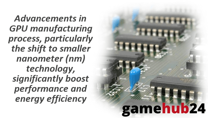
- Advances in nanometer technology are enabling the production of more powerful and energy-efficient GPUs.
- Increasing transistor density presents challenges in terms of heat dissipation and power consumption.
- The future of GPU manufacturing will be shaped by further advancements in nanometer technology and the development of new materials and techniques.
What is the role of silicon wafer production in GPU manufacturing?
The fabrication of silicon wafers is the foundation of GPU production processes. This procedure is essential because it creates the framework for the Graphics Processing Unit (GPU). A thin slice, or wafer, is made of silicon, a semiconductor. After that, this wafer serves as the foundation for the complex GPU production process. The final product’s performance and efficiency are directly impacted by the quality of the silicon wafer. Consequently, one of the most important steps in the manufacturing of semiconductors is the creation of high-quality silicon wafers.
How is semiconductor fabrication related to silicon wafer production?
The manufacture of silicon wafers is the first step in the complex process of fabricating semiconductors. The intricate architecture of a GPU is constructed on top of the silicon wafer. GPU’s complex circuits are created on the wafer using a variety of operations like etching, patterning, and depositing. As a result, the manufacture of silicon wafers is an essential stage in the fabrication of GPUs since they determine the ultimate product’s dependability and performance.
What is the importance of clean room technology in silicon wafer production?
The manufacture of silicon wafers depends heavily on clean room technologies. Dust and other impurities must be removed from the environment throughout the silicon wafer manufacturing process. A single dust particle has the ability to induce faults in the wafer, which raises production costs and reduces yield rate. As a result, high-quality silicon wafers are produced using clean room technology, which ensures a regulated environment for sophisticated GPU manufacturing processes.
Did you know that the GPU manufacturing process uses Extreme Ultraviolet (EUV) lithography, a revolutionary technology that makes chips smaller and more effective? Leading businesses like Nvidia, TSMC, and Intel are presently using this technology to create their cutting-edge GPUs.
What are the key steps in the GPU manufacturing process?
The creation of a silicon wafer is the first stage in the intricate process of producing a GPU, which concludes with the testing and packing of the finished product. Lithography, etching, doping, and ion implantation are the crucial processes. Each stage plays a critical role in determining the GPU’s efficiency and performance. The procedure calls for extreme control and precision, making it a difficult undertaking that only a select few businesses, such as TSMC and Nvidia, have successfully completed.
How does lithography contribute to GPU manufacturing?
A crucial step in the production of GPUs is lithography. It entails transferring a pattern from a photomask to the silicon wafer using light or other electromagnetic waves. To build a GPU’s intricate layers, this procedure is repeated numerous times. Extreme Ultraviolet (EUV) lithography has made the process more accurate, allowing for the creation of GPUs with smaller nanometer (nm) chips, which results in improved performance and energy efficiency.
What is the role of the photomask in the lithography process?
A key component of the lithography process used to manufacture GPUs is the photomask. It’s a plate with designs that match the GPU’s circuit design. The complex circuits of the GPU are created when light is projected through the photomask and onto the silicon wafer. A crucial step in the manufacturing of nanoscale GPUs, the photomask’s accuracy and precision directly affect the final product’s dependability and performance.
How does etching fit into the GPU manufacturing process?
Etching is a crucial step in the production of GPUs. A layer of photoresist is applied to the silicon wafer following the lithography process. The intended circuit layout is then removed by etching the wafer’s exposed photomask regions. High-performance computing is made possible by the intricate architecture that is created by repeating this procedure for every layer of the GPU. Etching is therefore a crucial stage in the sophisticated GPU production processes.
Advice: If you’re curious about the industry that produces GPUs, you should think about going to conferences like the GPU Technology Conference (GTC). It’s a fantastic chance to discover possible career prospects, network with industry leaders, and learn about the most recent developments in the field.
What is the purpose of doping process and ion implantation in GPU manufacturing?
Two important steps in the production of GPUs are doping and ion implantation. Doping is the process of introducing contaminants into a silicon wafer in order to change its electrical characteristics. In contrast, ion implantation involves the acceleration of ions and their implantation into the wafer to modify its properties. These procedures are essential for generating the p-n junctions that serve as the foundation for transistors, which are the GPU’s building blocks. As such, they have a big impact on how well and efficiently the finished product works.
How is the GPU performance tested and ensured?
There are several demanding tests involved in ensuring a GPU’s performance. Starting at the wafer level, these tests proceed all the way through to the packaging and final assembly phases. Defect detection, circuit functionality verification, and performance evaluation under various operating situations are all part of the testing process. Making sure the GPU satisfies the necessary requirements and can provide the anticipated performance in practical applications is the aim.
What is the significance of wafer testing in GPU manufacturing?
An essential stage in the production of GPUs is wafer testing. Prior to being cut and packaged, every chip on the silicon wafer is inspected for flaws. By identifying defective chips early in the production process, this method lowers waste and raises output rates. Wafer testing is essential to preserving the final product’s performance and dependability since it guarantees that only superior chips advance to the latter stages of manufacturing.
How does chip packaging affect the performance of the GPU?
A critical component of GPU production that has a direct bearing on the end product’s longevity and performance is chip packaging. It entails attaching the external circuitry to the chip while it is housed in a protective shell. In addition to shielding the chip from environmental elements and physical harm, packaging also helps with heat dissipation, which is essential for preserving the GPU’s longevity and performance. Therefore, a major factor influencing the GPU’s overall performance is the quality of the chip packaging.
What is the role of transistor density in GPU performance?
An important factor in influencing a GPU’s performance is transistor density. The processing capacity and energy efficiency of the GPU are directly impacted by the number of transistors crammed into a given area, which is measured in nanometers (nm). The GPU can process more calculations each cycle as transistor density rises, which improves performance. Nevertheless, increased transistor density also poses problems with power consumption and heat dissipation, which makes it a crucial component in GPU manufacture and design.
What does nanometer technology mean in the context of GPU manufacturing?
Nanometer technology, as it relates to GPU manufacture, describes the transistor sizes employed in the chip. More transistors may be crammed into a given space at a smaller size, expressed in nanometers (nm), which improves performance and energy efficiency. However, problems with heat dissipation and power consumption rise with decreasing size, therefore nanoscale technology plays a crucial role in GPU design and production.
How does nanometer technology impact microprocessor design?
The design of microprocessors is significantly impacted by nanometer technology. The processing capability of the microprocessor can be increased by designers by packing more transistors into a given area as their sizes shrink. But this also makes the design and production process more intricate, necessitating sophisticated methods and accuracy. Moreover, problems like heat dissipation and power consumption worsen with decreasing size, necessitating creative fixes to preserve the microprocessor’s dependability and performance.
What is the relationship between nanometer technology and integrated circuit design?
Integrated circuit design and nanotechnology are closely related fields. The integrated circuit’s performance and complexity are directly impacted by the transistors’ size, which is expressed in nanometers (nm). As the size gets smaller, the circuit’s processing capacity increases because more transistors can fit into a given space. But this also makes the design and production process more intricate, necessitating sophisticated methods and accuracy. Thus, integrated circuit architecture is going to be significantly shaped by nanotechnology.
How does die shrink relate to nanometer technology in GPU manufacturing?
In the semiconductor industry, the term “die shrink” refers to the technique of shrinking a chip’s transistor size, which is made feasible by developments in nanoscale technology. Reduced transistor size allows for more transistors to fit into a given space, boosting the GPU’s processing capacity and energy efficiency. Die shrink is a crucial component in the design and production of GPUs since, as size shrinks, power consumption and heat dissipation become more difficult to manage.
How does Moore’s law apply to GPU manufacturing?
For many years, the semiconductor industry has been guided by Moore’s law, which stipulates that the number of transistors on a chip doubles roughly every two years. This law has propelled the development of GPU manufacturing, resulting in the creation of GPUs that are both more powerful and energy-efficient. But when transistor sizes go closer to the atomic level, power consumption and heat dissipation issues become increasingly significant, pushing Moore’s law to its breaking point.
What is the impact of Moore’s law on yield rate in semiconductor manufacturing?
In semiconductor production, the yield rate is greatly impacted by Moore’s law. The manufacturing process becomes more difficult as the number of transistors on a chip doubles roughly every two years, increasing the likelihood of mistakes. This may cause the yield rate to drop, raising the production cost. Therefore, a major problem facing the semiconductor industry is to maintain a high yield rate while following Moore’s law.
How does Moore’s law influence thermal design power in GPUs?
The impact of Moore’s law on GPU thermal design power (TDP) is significant. The power consumption of the GPU rises along with its heat generation every two years as the number of transistors on a chip doubles. To control the heat and preserve the GPU’s dependability and performance, creative methods are needed. Thus, Moore’s law has a significant influence on how GPU manufacturers build their thermal and power management systems.
What is the effect of Moore’s law on power consumption in GPUs?
The impact of Moore’s law on GPU power usage is substantial. The GPU’s power consumption rises as a result of a chip’s transistor count roughly doubling every two years. To control the power and preserve the GPU’s dependability and performance, creative solutions are needed. As a result, Moore’s law has a significant influence on how GPU manufacturers design their power management techniques.
What are the future trends in the semiconductor industry for GPU manufacturing?
The unwavering quest for increased performance and energy efficiency is what propels the semiconductor industry’s continuous evolution. Future developments in nanoscale technology, the drive toward 3D integration, and the creation of novel materials and production processes are anticipated to influence the trends in GPU manufacture. These developments will keep pushing the envelope of what is conceivable, which will result in the creation of GPUs that are both more potent and energy-efficient.
How is the semiconductor industry evolving in terms of GPU manufacturing?
The fabrication of GPUs is one area where the semiconductor industry is fast growing. Nanotechnology developments are making it possible to produce GPUs that are both more powerful and energy-efficient. Concurrently, the industry is investigating novel materials and production methodologies to surmount the obstacles presented by the decreasing transistor dimensions. Future GPU manufacture is expected to be shaped by these advancements, resulting in the creation of GPUs that are both more powerful and energy-efficient.
What are the anticipated advancements in nanometer technology for GPU manufacturing?
The future of GPU production is anticipated to be driven by developments in nanoscale technology. New issues with heat dissipation and power consumption are arising as transistor sizes continue to decrease. The industry is investigating novel materials and production processes, such as 3D integration and the usage of novel semiconductor materials, in an effort to address these issues. Future GPU manufacture is expected to be shaped by these developments, resulting in the creation of GPUs that are both more powerful and energy-efficient.